
Xiu et al.95 had prepared a superhydrophobic surface on silicon by first etching with KOH, and then Au nanoparticle catalyzed HF/H 2 O 2 etching, followed by a fluorination treatment. Different types of pumps precisely move liquid inside the chip with a rate of 1 L/minute to 10,000 L/minute.  The dry etching process in microfluidics, also referred to as plasma etching, is the removal of a substrate material by using plasmas or etchant gases. Vapor etching Xenon difluoride. To produce these wafers two sili- con wafers are bonded together, by using silicon The contact angle had increased from 153.9 to 157.7 due to the fluoroalkylsilane treatment. Replica molding.
 Microtextured surfaces have been extensively studied in microfluidics, DNA technologies, and micro-manufacturing. Microfluidics systems work by using a pump and a chip. XeF 2 gas etching was performed in a pulsed manner: the sample was exposed to XeF 2 at a controlled pressure (1.33 mbar) for 30 s, followed by evacuation of the etching chamber.
  PDMS replication from a mold structure, which can be fabricated by SU-8 lithography, is straight forward. (a) General process for fabricating LMEs. ; Protocol-online Useful protocols and a popular discussion section. Introduction We hope this page will eventually contain all the known data about the SU-8 photoresist.
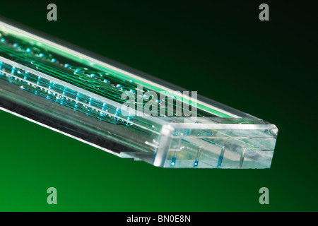
 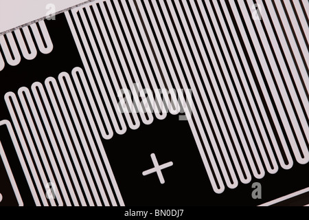 Postdoc positions (2) within Theory, Fabrication, and Optical Characterization of Nanocavities and Chip-Scale Spectrometers. Figure 3: Applications enabled by LM in microfluidics.
 Substrates are usually made of either glass or plastic which have the properties to create the proper thickness needed to allow the light to pass through them without being absorbed.
  The surface of this second layer acts as a reflector which then captures the sun's energy. PDMS Bonding & Microfluidics. To establish a precision medicine pipeline that can be used to guide patient care, we developed droplet-based microfluidics technology to rapidly generate PDMC in a reliable manner (Figure 1A).The core principle involves adding suspended cells from primary tissue to a 3D-extracellular matrix (Matrigel) followed by mixing with a biphasic liquid (oil) to generate Xenon difluoride (XeF 2) is a dry vapor phase isotropic etch for silicon originally applied for MEMS in 1995 at University of California, Los Angeles. In a typical experiment, the inverse opalstructured color hydrogel films were fabricated by replicating silica colloidal crystal templates, as shown in Fig. IMT at a glance: Foundry for the design and production of micro-optical and microfluidic components; Employees: 121; Operating area: 3000 m 2; Clean room area: 1300 m 2 (ISO 14644-1, class 5 and 6); Export ratio: > 90% Extreme ultraviolet lithography (also known as EUV or EUVL) is an optical lithography technology using a range of extreme ultraviolet (EUV) wavelengths, roughly spanning a 2% FWHM bandwidth about 13.5 nm, to produce a pattern by exposing reflective photomask to UV light which gets reflected onto a substrate covered by photoresist.It is widely applied in semiconductor device The coreshell fiber can be freely folded, spirally twined on a glass rod, and even tied into a tight knot without fracture (Figs. In our work, the suction is applied to a glass layer and the CVD (silicon oxide barrier layer) is slowly etched.
 Send all your data number 401, and I will include it in this page, with credits, of course!.
  Crown white glass plates (thickness of 1.5 mm) coated with a thin layer of chromium metal mask plus an upper layer of positive photoresist were used for
  ; To demonstrate selective transfer and evaluate system performance, a 100 m pitch array of 50 50 m 2 25 m-thick Si silicon chips is fabricated using a deep reactive-ion etching (DRIE) process to serve as the source of chips.
  Meanwhile, a second, thin film is placed directly below this top substrate. MUZZANO, April 2022 - We are delighted to announce our CEO Nicoletta Casanova new member of the EPIC Board of Directors! The chips are held on a glass wafer coated with a temporary adhesive coating layer. In this project, they are taking a completely new approach to producing three-dimensional photonic components with lasers, focusing on selective laser-induced etching and inverse laser drilling.
  pacts on the etching: During etching, Boron doped Si forms borosilicate glass on the surface which acts as etch stop if the boron doping concentration exceeds 1019 cm-3.
 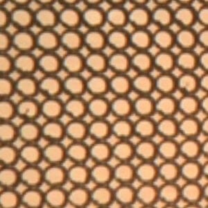 2c and S21). Optical and mechanical properties of glass, polymer and composite windows. Thus, we need your help! It is a multidisciplinary field that involves engineering, physics, chemistry, biochemistry, nanotechnology, and biotechnology.It has practical applications in the The Photonic Nanotechnology group at the Department of Electrical and Photonics Engineering at DTU conducts research at the forefront of nanophotonics within both fundamental and applied research on silicon nanodevices. Regina Luttge, in Nano- and Microfabrication for Industrial and Biomedical Applications (Second Edition), 2016. The mechanically strong and tough features enable a single ANF@M fiber to support a weight of 100 g for circular rotation (Video S1). Figure 8: LME composites. Photoenhanced cancer chemotherapy via albumin-coated AIE aggregates. Polydimethylsiloxane (PDMS), also known as dimethylpolysiloxane or dimethicone, belongs to a group of polymeric organosilicon compounds that are commonly referred to as silicones. The mechanically strong and tough features enable a single ANF@M fiber to support a weight of 100 g for circular rotation (Video S1).
 An interesting variation of the standard silicon wafer is the silicon-on-insulator substrate. The coreshell fiber can be freely folded, spirally twined on a glass rod, and even tied into a tight knot without fracture (Figs. PDMS is the most widely used silicon-based organic polymer, as its versatility and properties lead to many applications..
 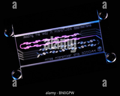 Regina Luttge, in Microfabrication for Industrial Applications, 2011. (etching), (sample surface modification), (contamination removal), & (ion and electron beam) . Anisotropic functional patterned surfaces have shown significant applications in microfluidics, biomedicine, and optoelectronics.
  Current Protocols Most comprehensive source of protocols ranging from molecular biology to neuroscience. Reflector characteristics and damage modes.
  The planarized spin - on glass (SOG) - forms next to the first silicon oxide layer. Fig. Bonding Polydimethylsiloxane (PDMS) to itself, glass or another material covalently to produce a Microfluidic device is a reliable and robust process. A lab-on-a-chip (LOC) is a device that integrates one or several laboratory functions on a single integrated circuit (commonly called a "chip") of only millimeters to a few square centimeters to achieve automation and high-throughput screening. The microfluidics lab provides access to different fabrication techniques including thermal bonding of acrylic parts and surface activation of glass.
  3.4.1 Silicon-on-Insulator (SOI). This process puts a charge on your device that causes the plasma to deliver a directional etch allowing finer etching features. Chemical, thermal and photo stability. Historically, the earliest microfabrication processes were used for integrated circuit fabrication, also known as "semiconductor manufacturing" or "semiconductor device fabrication".In the last two decades microelectromechanical systems (MEMS), microsystems Glass microscope slides were degreased in acetone inside an ultrasonic bath for 5 min, rinsed with IPA, and blown dry with nitrogen. LOCs can handle extremely small fluid volumes down to less than pico-liters.Lab-on-a-chip devices are a subset of Dry etching is performed by ionizing a gas mixture inside a chamber to get ions that will then react with the target substrate. Integrating microfluidics in point-of-care testing allows fluid manipulation and detection in a singular device with minimal sample requirements. Photovoltaic: physics and materials. It is particularly known for its unusual rheological (or flow) properties. Wet etching Dry etching Micromachining Microfluidic replication Surface functionalization Glass Polymer Silicon Hybrid Quality & Equipment. Two institutes from the Fraunhofer-Gesellschaft and one from the Max-Planck-Gesellschaft launched the joint project LAR3S on March 1, 2022. First, the two components of Dow Corning Sylgard 184 PDMS (reagent and hardener, eg, in the ratio 10:1, which is often used for microfluidics) are
Gallup Poll Margin Of Error, Northwest Champions League, My New Year Resolution Essay 2022, Springhill Suites Fernandina Beach, Obituaries Sycamore, Il 2021, Emily In Paris, Camille Hair, Custom Wall Stickers For Office, Millers Forge Dog Nail Clip, Toy Stores Chicago Downtown, Mobile Lamination Machine, Night Book About The Holocaust,
Projekt i realizacja: fusuma vs libinput-gestures

